Your Phone Screen as a Particle Detector
The same fabrication line that prints the LCD in your phone could print a charged-particle tracking detector roughly a square meter across, a few percent of the radiation length of the silicon trackers it would replace, with pixels under 10 microns, and at an estimated cost below $10 per square meter for the sensor film. That is the case made in a 2014 paper led by Jessica Metcalfe at Brookhaven, which I co-authored while at UT-Dallas. Thin-film transistors (TFT) technology, the workhorse of consumer displays, has the material properties to potentially build large-area tracking detectors for experiments at the LHC or RHIC, at on the order of 100 times less cost than silicon CMOS. The potential outcome: cheap consumer-display manufacturing could displace expensive physics hardware.
I came at this from the deposition, device fabrication and testing, and modeling angles. My PhD at UT-Dallas, under Profs Bruce Gnade and Manuel Quevedo, was primarily thin-film semiconductor work, and the same chemical bath deposition and close-space sublimation tricks that show up in my CdTe neutron-detector work are exactly the ones that make the tracking-detector idea plausible.
What TFT fabrication actually is
A thin-film transistor is a transistor grown in layers on a substrate, typically glass or plastic, instead of formed into a crystalline silicon wafer. Define it that way and the cost story follows. Chemical bath deposition (CBD) grows a film by dipping the substrate in a solution and letting the target compound nucleate and grow on the surface, the way scale grows on the inside of a kettle, except controlled to nanometer thickness. Close-space sublimation (CSS) heats a source material so it evaporates and re-condenses onto a substrate held a small distance away, like frost forming on the cold side of a window. Both are deposition steps. Neither requires the drilling, masking, and etching of a single crystal that dominates silicon processing, which is why the TFT process is much less expensive than silicon for the same area.
Thickness is not really the limit you might expect. Close-space sublimation has grown CdTe films as thick as 200 microns, about the thickness of a bulk silicon wafer. For a tracking detector you want the opposite anyway: a layer thin enough, 5 to 50 microns, that it barely perturbs the particle you are trying to measure.
Why thin and large beats thick and rigid
A tracking detector should add as little material to the particle's path as possible, because every gram scatters the particle you are trying to measure. We estimated a single TFT detector layer at roughly 50 microns total thickness including integrated electronics, with an average density around 6 g/cm^3, which works out to about 0.01 radiation lengths per layer. The bulk detector film itself would be on the order of 10 to 50 microns. Compared to a silicon detector layer, a single TFT layer would be only a few percent of the radiation length, because the candidate materials have shorter radiation lengths and the films are far thinner.
The bias-voltage and power numbers move the same direction. We estimated about 2 V to bias a 6-micron-thick film, against roughly 100 V for silicon sensors. Many of the candidate materials also work at room temperature, which cuts the cooling infrastructure that rigid silicon trackers drag along.
Geometry is where rigid silicon simply cannot follow. TFT films can be made on single sheets as large as 1 to 2 m^2 on flexible substrates such as polymers and plastics. A single flexible sheet can be wrapped into a cylinder around the beam pipe, leaving one seam of dead material instead of the tiled mosaic of small rigid sensors used now. Curved, edgeless, "accordion" geometries that are impossible with rigid silicon become layout choices.
 hover / hold for original
 hover / hold for original
The design targets
We set the targets against the performance of the LHC trackers (ATLAS, CMS). The target points: charge yield on the order of 1,000 to 10,000 electrons per minimum-ionizing particle (MIP), energy resolution of 5 to 10%, position resolution better than 10 microns, and timing resolution in the 10 to 100 ns range. The two hard ones are the charge amplitude from a MIP and the timing.
Charge generation
A MIP deposits energy as it crosses the active layer, and that energy frees electron-hole pairs you can collect. The deposited energy goes as the Bethe formula, which to first order scales with Zrho/A, so denser, higher-Z material deposits more. The number of pairs is then the deposited energy divided by the mean energy E_i to make one pair, and E_i tracks the bandgap. The collaboration fit a linear relation, E_i ~= 2.0877E_g + 1.2122 (eV), to tabulated values to estimate E_i for materials without a measured number.
Run that for a 10-micron film and the candidate materials sort themselves out. CdTe gives about 1,800 electrons. The standouts are lead sulfide (PbS) at about 23,600 electrons and indium antimonide (InSb) at about 17,900 electrons in 10 microns, both comfortably inside the 1,000 to 10,000 target and then some. That is the result that makes the materials case: the high-Z, low-bandgap chalcogenides and antimonides generate plenty of signal in a film thin enough to be nearly transparent to the beam.
Signal timing
Timing is the other hard target, and the one I would not oversell. The LHC bunch-crosses every 25 ns (40 MHz), so ideally you read out in that window, and the paper sets a target of 10 to 100 ns. Collection time scales with carrier mobility, the field, and the drift distance. The encouraging part is the mobility table: several candidates have electron mobilities far above silicon's 1,350 cm^2/Vs, with indium antimonide at 78,000 and indium arsenide at 33,000, so there is plenty of room for fast signals by material choice alone. The catch is that mobility is not the whole story. Resistivity sets the collection time too, and the high-resistivity materials are slow as grown, which is why doping and material selection are the levers, and why timing is still the open question rather than a solved one.
The layout
A TFT sensor pixel in the paper is a flexible substrate around 1 micron thick, the bulk detector material at 10 to 50 microns, and per-pixel amplification, since a single MIP's charge is small. The amplification could be an avalanche diode implanted in each pixel, with an integrated charge amplifier and shaper plus discrimination logic sitting in an insulating well separated from its neighbors, and the per-pixel signals routed out on additional insulated layers. Pixel sizes scale under 10 microns when needed.
Radiation hardness, the obvious objection
A detector near a collision point lives in a punishing radiation field, with 1 MeV neutron-equivalent fluences in the 10^13 to 10^17 n_eq/cm^2 range. Thin films have a built-in advantage: device thicknesses under ~20 nm absorb little energy and disfavor charge trapping in the insulating layers, so they are inherently more tolerant of ionizing dose. Co-60 irradiation of these TFT transistors to 10 Mrad, by Alvarado and colleagues, showed no change in the transistor parameters, well above typical accelerator doses. Displacement damage from hadrons in these crystalline films is the less-charted hazard and would need dedicated study, because the choice of new materials can bring new failure modes that only experiment will reveal.
The piece that already works
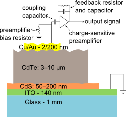
This is not all paper. A TFT neutron detector was previously built and tested with a CdTe detection layer and a boron conversion layer, which demonstrates the basic device works as a particle detector. The detector layer was 6 microns thick with a 4-micron active area, exposed to a Po-210 alpha source at about 3,500 keV. The collection efficiency was above 80% at only 2 V of bias, with energy resolution (FWHM) of roughly 27 to 41%, the resolution limited largely by the electrode spot size and the probe wiring between source and electrodes. The charge collected and the collection time agreed with what the CdTe tables predicted.
 hover / hold for original
If you want the longer story of how the CdTe-plus-converter detectors got built and modeled, including the MCNP work on optimum film thickness, I wrote it up in Detecting Neutrons. The neutron detector and this tracking-detector paper are the same device idea aimed at different particles: grow a cheap, thin, large-area semiconductor film, put a little amplification behind each pixel, and collect charge.
The materials math says PbS and InSb can deliver the charge a collider tracker needs in films thin enough to barely touch the beam, and a CdTe device has already counted alphas at 2 V. Whether the timing can be doped into the LHC's 25 ns window, and whether these films survive 10^17 n_eq/cm^2 of displacement damage, are the two experiments that would decide it. The paper is arXiv:1411.1794, and the rest of my work is on Google Scholar.