Liquid Semiconductors That Heal Themselves
An alphavoltaic is the alpha-particle analog of a solar cell. You put an alpha emitter against a semiconductor junction, the alpha generates electron-hole pairs in the depletion region, and the junction collects them as current. The reason you would bother is energy density. Alphas carry roughly an order of magnitude more energy per decay than betas, so on a specific-energy versus specific-power chart the alphavoltaic region sits up and to the right of everything else, betavoltaics included, out past 10,000,000 Wh/kg in the long-discharge corner. The catch has always been that you cannot collect that energy for long before the semiconductor is full of holes, metaphorically and literally.
The single thing that kills a high-power-density alphavoltaic is the alpha particle itself. An alpha carries a few MeV and deposits it over a short range, and a good fraction of that energy goes not into electron-hole pairs you can collect but nuclear interactions that knock atoms off their lattice sites. Those displacements pile up and create electronic defects. A solid alphavoltaic is therefore a device that destroys its own collecting medium as it runs, and no solid semiconductor has been shown to withstand sustained alpha bombardment without severely degrading. That is the central blocker for the whole class of devices.
One possible workaround is to use a semiconductor that has no fixed lattice to damage. A liquid. In a liquid semiconductor a displacement event has nothing permanent to displace. The atoms are already mobile, so a knocked atom diffuses back into a low-energy configuration on a timescale far shorter than the device lifetime. The defects anneal away as fast as the alpha makes them. I like the phrase "self-healing" for this because it is literally what is happening, the medium repairs the damage continuously rather than accumulating it.
This is not just an argument on paper. A 2018 report in Scientific Reports (Nullmeyer, Kwon, et al.) ran a liquid selenium-sulfur alphavoltaic and saw no measurable degradation for a dose equivalent to a year of 2.5 Ci of 5.3 MeV alphas, where solid SiC and InGaP comparison cells lost most of their collection efficiency over the same span at far lower fluence. SiC fell off a cliff at He fluence around 1.05e12 MeV/cm^2 and InGaP at 6.8e13 MeV/cm^2, while the liquid Se-S held flat out to 2.68e14 MeV/cm^2. That is the result that made the liquid route worth chasing, because it converts "self-healing" from a hopeful mechanism into a measured degradation curve that stays flat where the solids collapse.
Selenium-iodide as the eutectic
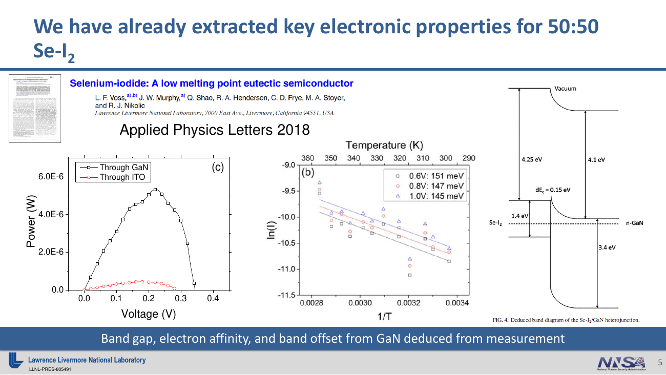
The group I joined at LLNL, Rebecca Nikolic's group, worked on a similar selenium-iodine liquid alloy. Selenium is already a semiconductor and it has a long history in photoconductors, but pure selenium melts around 220 C, which is hotter than you want for a device you intend to keep molten. Alloying it down is the trick. We characterized a 50:50 selenium-iodide eutectic and published it as "Selenium-iodide: A low melting point eutectic semiconductor" (Voss, Murphy, et al., Applied Physics Letters, 2018).
The point of the eutectic is the melting point. A lower melting point means you can run the liquid at a milder temperature, and milder temperature helps with improved carrier mobility and lower dark/generation current in a device that has to actually produce power. The ultimate goal with these devices is to produce enough heat from your radioactive source to keep the whole thing liquid, which the eutectic also helps with. The two design goals were exactly that, push the melting temperature down further, and find a way to keep the material molten in service.
 hover / hold for original
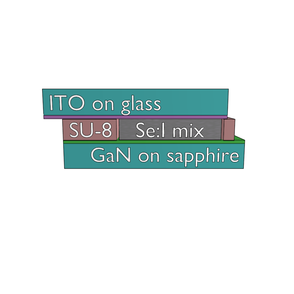
We built the eutectic into a GaN / Se:I2 / ITO heterojunction to measure it. The n-GaN gives a known, well-behaved partner to form the junction against, and the indium-tin-oxide top contact is transparent, so we could illuminate the Se:I with UV through it and measure photopower without an actual alpha source in the loop. From the temperature dependence of the current-voltage curves the group deduced the key electronic properties: a bandgap of about 1.4 eV for the 50:50 Se-I2, an electron affinity around 4.1 eV, and a conduction-band offset to GaN of about 0.15 eV. A 1.4 eV gap is right in the range you want for energy conversion, close to silicon and to the GaAs-class photovoltaics, which is part of why selenium is a reasonable choice rather than an exotic one.
 hover / hold for original
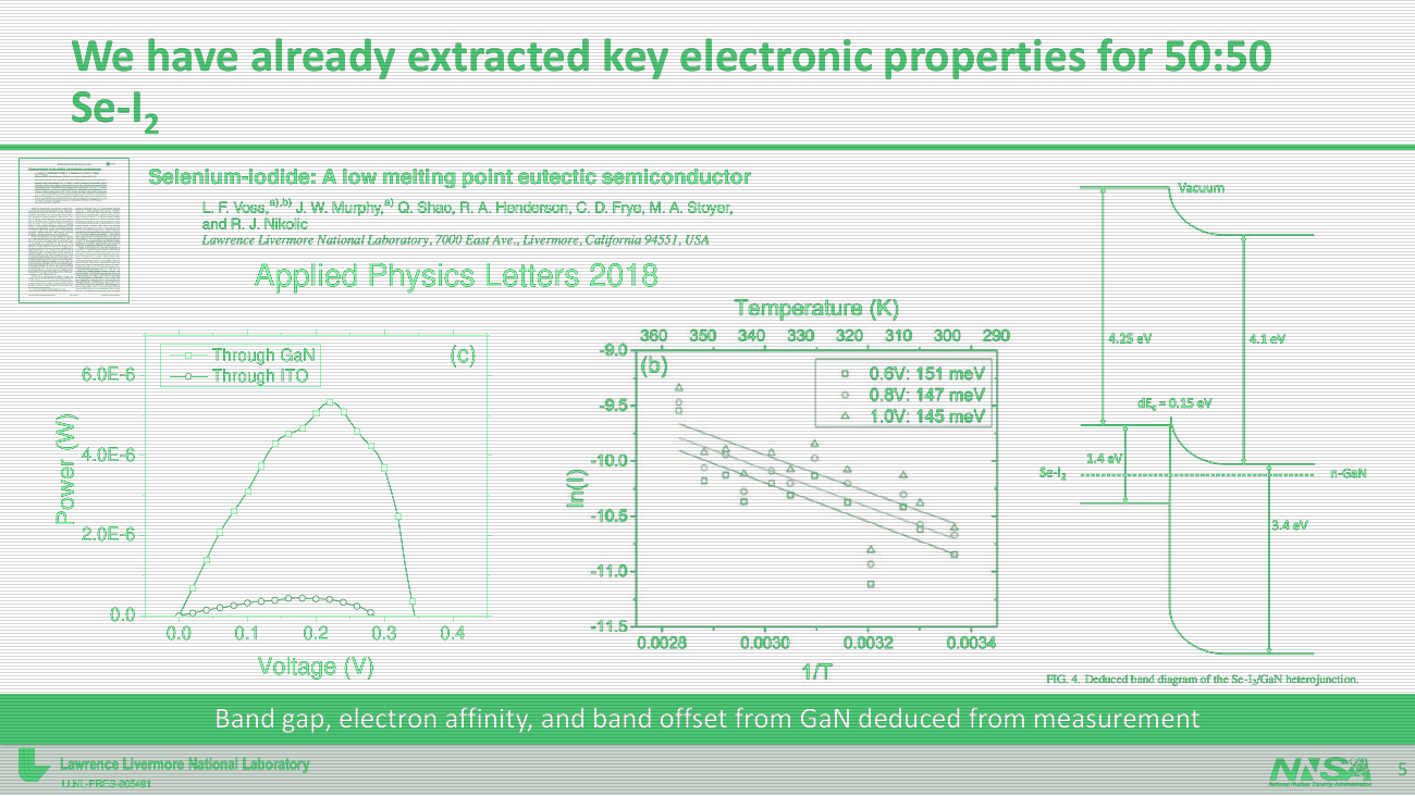
The cleanest piece of evidence for the whole concept showed up when we swept the device through the melting point. Power generation continued across the solid-to-liquid transition with no abrupt change in behavior. The open-circuit voltage decreased with increasing temperature, as you would expect, but the fill factor improved and the ideality factor got better, and there was no discontinuity where the material melted. The device works as a semiconductor junction whether the selenium-iodide is solid or molten. That is the experimental permission slip to run it as a liquid on purpose.
Letting the source melt its own semiconductor
If the device has to be molten to self-heal, something has to supply the heat, and carrying a heater into a sealed radioisotope battery defeats the point. The elegant version is to let the alpha source heat its own semiconductor. An alpha emitter is a heat source by definition, that is the same decay power an RTG harvests, so the question is whether the decay heat alone can hold the selenium-iodide above its melting point.
The group's thermal modeling says yes, for the right isotope and loading. For Pu-238 (half-life 87.7 years) the calculation shows that roughly 6 percent actinide loading in the Se-I is enough to reach the melting point, versus around 45 percent for Am-241 and a small fraction of a percent for the very hot Po-210. The Pu-238 number is the interesting one because Pu-238 is the workhorse alpha source for space power and its heat output per gram is well matched to this job. The conceptual device the group sketched was a 20 um thick Se:I layer on a 200 um substrate, loaded around 10 vol% Pu-238, at an estimated 5 percent conversion efficiency and roughly 1.6 mW/cm^3 per chip. Those are early projections at TRL 1 and I would not bank on the exact numbers, the modeling assumptions drive them, but the self-heating mechanism itself follows directly from the decay power and the melting point and does not require anything to go right beyond the thermodynamics.
What I find satisfying about this concept is that the failure mode of every solid alphavoltaic, the relentless dumping of alpha energy into the lattice, becomes the enabling feature here. The same energy that would destroy a crystal instead keeps the liquid liquid, and the liquid heals the damage the alphas would otherwise cause. The damage budget and the heat budget point in the same direction for once.
The liquid alphavoltaic was one of three radioisotope-battery concepts the group pursued, alongside high-aspect-ratio 3D betavoltaics and gas-scintillator alphavoltaics. I wrote up the broader picture, and where I fit in it, in Radioisotope Batteries. The selenium-iodide paper and the rest of the LLNL-era work are on my Google Scholar.