An Eight-Month Nuclear Battery Experiment
We built the first high-aspect-ratio, three-dimensionally structured betavoltaic, filled it with a promethium-147 source, and ran the highest-activity device for eight months. It put out about 200 nW at the start, and over the run its output fell off in step with the radioactive decay of Pm-147. That last sentence is the whole point of the experiment, so it is worth being precise about what it means and how we got there. This is the device demonstration paper that followed the radioisotope battery work I did at LLNL in Rebecca Nikolic's group, where I ended as co-PI on the project; I was first author on this one, with the fabrication, source filling, and the long-term measurement campaign as my piece of it.
A betavoltaic is a semiconductor diode with a beta emitter sitting against it. The beta particles ionize the semiconductor and create electron-hole pairs, the built-in junction sweeps that charge out, and you get a current. It is the same physics as a solar cell, except the source is radioactive decay instead of sunlight, so the output does not depend on whether the lights are on, it depends on how much radioactive material you have and how fast it is decaying. The catch is geometry. A flat source on a flat diode wastes about half its betas to the wrong hemisphere, and the source layer you can fit on a flat surface is thin. The fix is to go three-dimensional: etch deep trenches into the silicon and pack the source down into them, so far more source sits next to far more active semiconductor per unit of chip footprint.
The diodes we used were ridged silicon PIN structures from Radiation Detection Technologies, with a ridge width of about 17 microns, a ridge spacing of about 22 microns, and a depth of 450 microns. That is an aspect ratio up to about 40, meaning the trenches are roughly forty times deeper than they are wide. Each diode was about 1 by 1 cm. The conformal p+ junction on these is no thicker than about 200 nm, and that thin highly-doped skin is what I have been calling the "dead layer": charge generated inside it recombines before the junction can collect it, so any beta energy deposited there is lost. The dead layer matters because it sits directly between the source and the active region, so the source's lowest-energy betas pay a toll before they ever reach the part of the device that counts.
Getting the source into the trenches
Filling 450-micron-deep, 22-micron-wide slots with a radioisotope is the hard part, because surface tension does not want to pull liquid down into a slot that narrow. We used a modified drop-casting technique. Dip the chip in pure ethanol so the trenches wick full, lay it face up so a meniscus of liquid sits on the surface held by surface tension, then pipette 20 to 40 microliters of aqueous Pm-147 chloride onto that ethanol and let it mix in by diffusion. After the top dried we baked the chip at 50 C to drive out the remaining ethanol and water. We developed the recipe on a non-radioactive analog, neodymium chloride, before doing it with the real source, and cross-sectional SEM of the mock devices showed the chloride going down into the ridges rather than sitting on top.
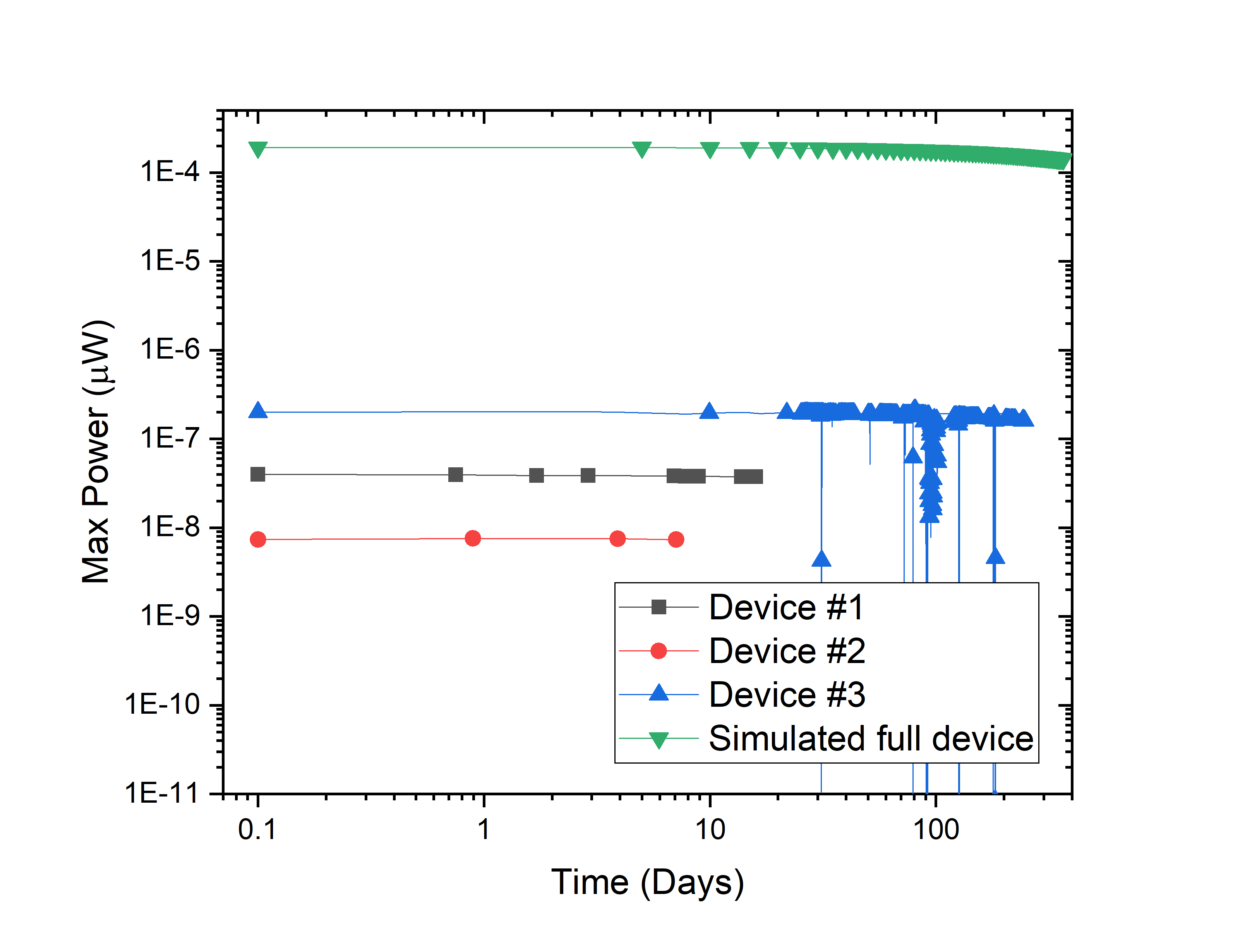
We made three devices, with Pm-147 activities of 2.4, 7.4, and 29.5 mCi, which we determined by gamma counting at the end of testing. The two figures of merit at the start were the short-circuit current and how it compared to the theoretical maximum. The theoretical max assumes every beta deposits all its energy in the active silicon at 3.61 eV per electron-hole pair, with nothing lost to the dead layer or to geometry. If the source sat only on the top surface, isotropic emission alone would throw away about half the betas and cap you near 50% of that maximum. Our three devices came in at 68, 74, and 77% of theoretical max. Being well above 50% is the evidence that the drop-casting actually infiltrated the source down into the trench volume rather than leaving it on the surface, which is the thing the whole 3D approach depends on. The highest-activity device produced 200 nW at the start, with a short-circuit current of about 2 microamps, an open-circuit voltage of 170 mV, and a fill factor of 59%.
Eight months of watching it decay
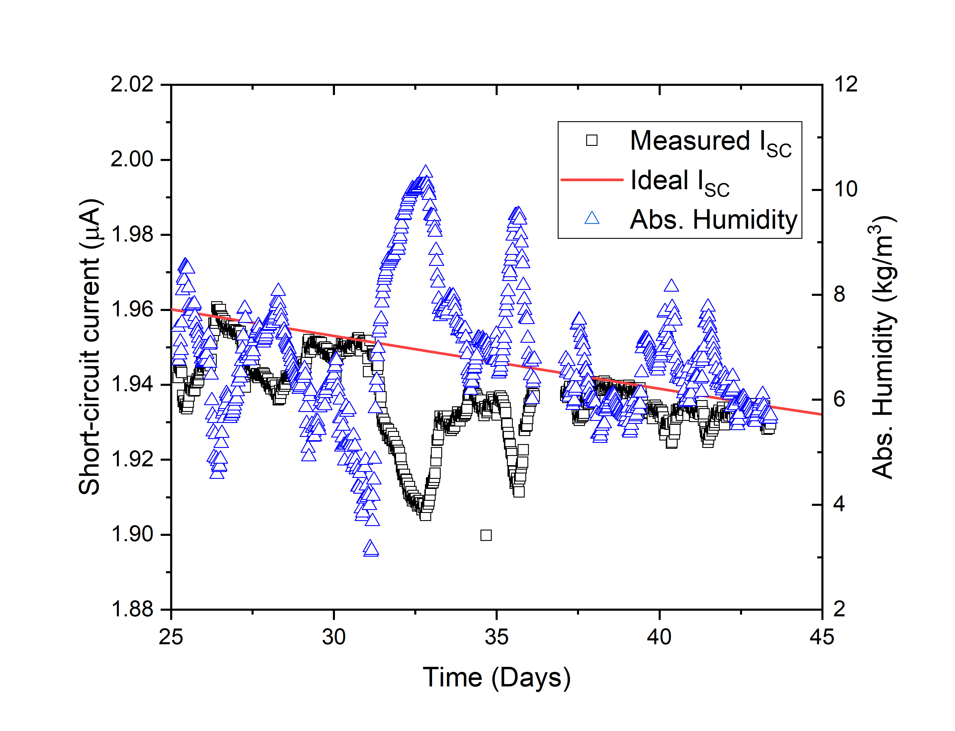
We logged the highest-activity device for over eight months. The short-circuit current dropped from about 2 to 1.67 microamps over 246 days. Pm-147 has a half-life of about 2.6 years, and decaying the starting current over 246 days predicts 1.673 microamps. So the measured falloff and the radioactive decay agree to within the last digit we can read. That agreement is the result I care about most, because it says the device is not quietly dying of anything other than its source running down. If alpha-emitting impurities in the Pm-147 had been building deep-level traps in the silicon, or if the betas themselves had been damaging the lattice, the current would have fallen faster than the half-life. It did not, so within the eight-month window there is no measurable radiation damage on top of ordinary decay.
 hover / hold for original
The few-percent wobble was the weather
On top of the clean decay there was a small extra wiggle in the short-circuit current, a few percent, that the half-life alone did not explain. To chase it down I put a temperature and humidity logger at the front of the fume hood where the measurements were running, and converted the readings to absolute humidity. The short-circuit current varied inversely with absolute humidity: when the room got more humid, the current dropped, and when it dried out, the current came back. The cause is that the source material is Pm-147 chloride in its hexahydrate form, which is hygroscopic, meaning it pulls water out of the air. On a humid day the source takes up extra water, and that water sits between the source and the silicon and attenuates the lowest-energy betas slightly before they reach the active region, which shaves a little off the current. It is a real-world measurement artifact, not a device defect, and it shows up as the source surface responding to the weather in the room.
 hover / hold for original
What it does and does not show
What we showed is that the first 3D-structured betavoltaic works, that you can fill high-aspect-ratio silicon with a real radioisotope and collect most of the charge you would predict, and that the device runs for eight months with no degradation beyond the decay of its own source. What it does not yet show is high power. 200 nW from a 29.5 mCi device is a long way from useful, and the reason is fill density: the drop-cast chloride only partially fills the trench volume. MCNP6 simulations of a fully filled device put the output near 192 microwatts, about three orders of magnitude higher, which would take roughly 11,000 mCi of source. Getting there means a denser, more promethium-rich fill, something like Pm2O3 instead of the hydrated chloride, and tuning the ridge width and spacing to balance power density against collection efficiency.
The full paper is "Demonstration of a Three-Dimensionally Structured Betavoltaic" in the Journal of Electronic Materials (2021); the rest of the LLNL-era papers are on my Google Scholar.