Silicon Beats Silicon Carbide (for Betavoltaics)
Planar 4H-SiC diodes lost 45% of their output power after 100 keV electron irradiation at a fluence of 1.32 x 10^18 cm^-2. Over the same kind of exposure, 3D silicon p-i-n diodes showed no measurable power drop out to 7 x 10^18 cm^-2, more than five times the fluence. For a Pm-147 betavoltaic, that result says silicon is the more radiation-hard semiconductor, which is the opposite of what the conventional wisdom predicts. This is the headline from our paper Radiation hardness of Si compared to 4H-SiC for betavoltaics assessed by accelerated aging using an electron beam system, out of Rebecca Nikolic's group at LLNL.
A betavoltaic is a battery that converts beta decay directly to current. You put a beta emitter against a semiconductor junction and the betas generate electron-hole pairs that the junction collects, the same physics as a solar cell with beta particles instead of photons. For a long-lived, microwatt-class power source, Pm-147 is a good emitter: 2.6 year half-life, a specific power density of 2.4 W/cm^3, and an average beta energy of 62 keV (endpoint 225 keV). I wrote up the device family and the isotope tradeoffs in Radioisotope Batteries, if you want the wider context.
The wide-bandgap intuition, and where it breaks
The standard reasoning goes like this. Wide-bandgap semiconductors (SiC, GaN, diamond) have lower leakage current, higher open-circuit voltage, and they are generally believed to be less prone to radiation damage. 4H-SiC has a 3.23 eV bandgap and a mature growth and fabrication base, so on paper it looks like the right converter for a betavoltaic. The catch is what "radiation damage" means here. The damage that kills a betavoltaic is displacement damage: a beta particle knocks an atom out of its lattice site, leaving a vacancy. Those vacancies cluster into deep-level states that trap or recombine the carriers you are trying to collect, and your output power drops.
Whether a beta can do that comes down to the displacement threshold energy, the minimum energy needed to dislodge a given atom. SiC has two sublattices, carbon and silicon, and they are not equally tough. The experimentally reported threshold to knock a carbon atom from its site is 17 eV; for silicon it is 24 eV. Plug those into the non-relativistic head-on collision formula for the incident electron energy and you get the key numbers: it takes about 88 keV of electron energy to displace carbon, and about 250 keV to displace silicon (in either material). That carbon site is the weak link. It is the lightest atom in the lattice and the easiest to knock loose.
Now line that up against the Pm-147 spectrum. The average beta is 62 keV, below the 88 keV carbon threshold, but the spectrum is broad and roughly 30% of the emitted betas carry more than 100 keV, comfortably above it. So a meaningful fraction of a Pm-147 source's own betas can displace carbon in SiC, but essentially none of them can displace silicon. Silicon has only the one, tougher sublattice. That is the whole inversion in one sentence: SiC has a soft spot that Pm-147 can reach, and silicon does not.
 hover / hold for original
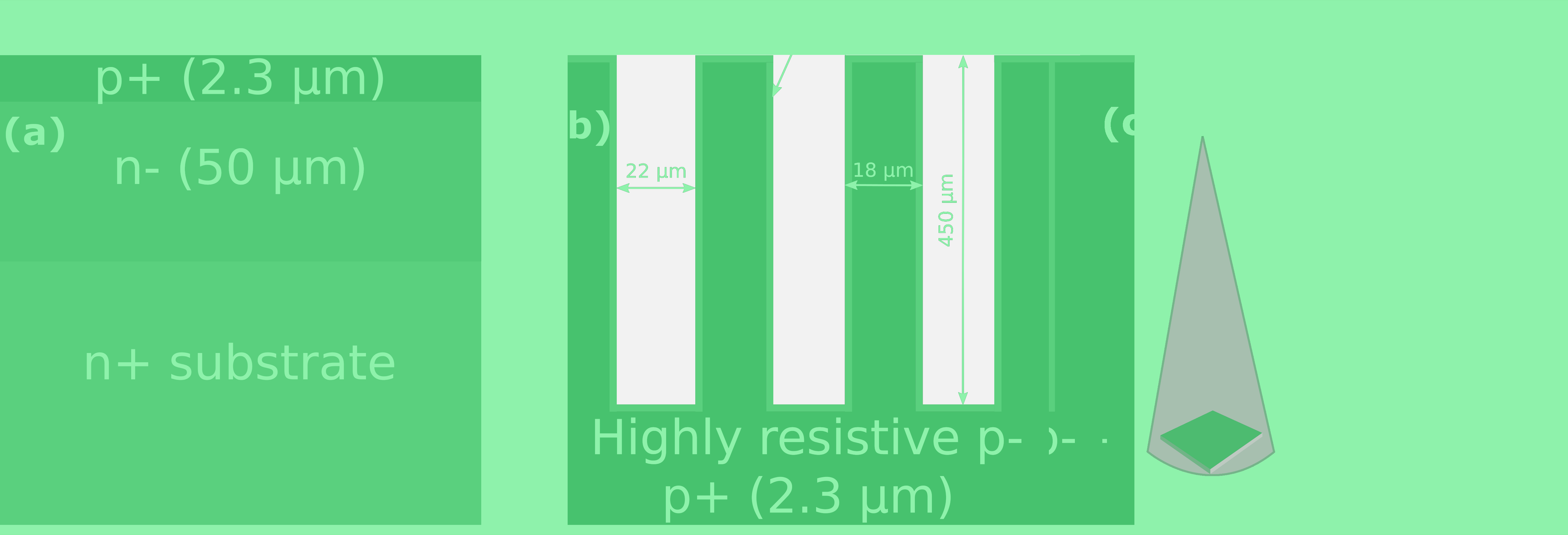
An electron beam as a beta surrogate
Testing radiation hardness the honest way means irradiating the diode with the real isotope and watching it for a long time. We did that too: a 1 mCi Pm-147 foil placed 2 mm from a SiC diode for 125 days delivered a cumulative beta fluence of 2.3 x 10^14 cm^-2, and there was no power degradation. That confirms SiC survives Pm-147 at the 10^14 cm^-2 scale, but it tells you nothing about the lifetime fluence a real battery accumulates, and waiting years per data point with a high-activity source is neither fast nor safe.
So the group used a custom electron beam system (built by Kimball Physics) as a beta-particle surrogate. The energy is tunable from 1 to 100 keV, which covers the full beta spectrum of tritium and Ni-63 and roughly 70% of the Pm-147 spectrum. The trick is flux. We ran the beam at an electron flux of 8 x 10^13 cm^-2 s^-1, about 2 x 10^6 times the flux from the 1 mCi Pm-147 foil. That compresses years of aging into hours. A fluence of 1 x 10^18 cm^-2, which would take an impractically long dwell under a real source, takes under 2 hours on the beam. The whole rig sits in a lead-lined cabinet rated for 150 keV x-ray protection, so there is no radioisotope handling at all during the accelerated test.
There is a control buried in that approach, and it matters. We irradiated a SiC diode with 62 keV electrons (the Pm-147 average) to a fluence of 3.15 x 10^17 cm^-2 and saw no power drop. 62 keV is below the 88 keV carbon threshold, so nothing gets displaced, and the device is fine even at high fluence. The damage only shows up when the electron energy crosses the threshold.
What broke, and what did not
When we took the same SiC device family up to 100 keV, above the carbon threshold, the 45% power drop appeared at 1.32 x 10^18 cm^-2. The energy dependence is the tell. No damage at 62 keV, clear damage at 100 keV, with the crossover sitting right where the carbon displacement threshold says it should. We attribute the degradation to carbon-vacancy-related defects (the Z1/Z2 and EH6/EH7 centers known to act as recombination traps), produced once the electrons get energetic enough to dislocate carbon. The experiment puts the carbon displacement threshold between 62 and 100 keV, consistent with the calculated and previously measured values.
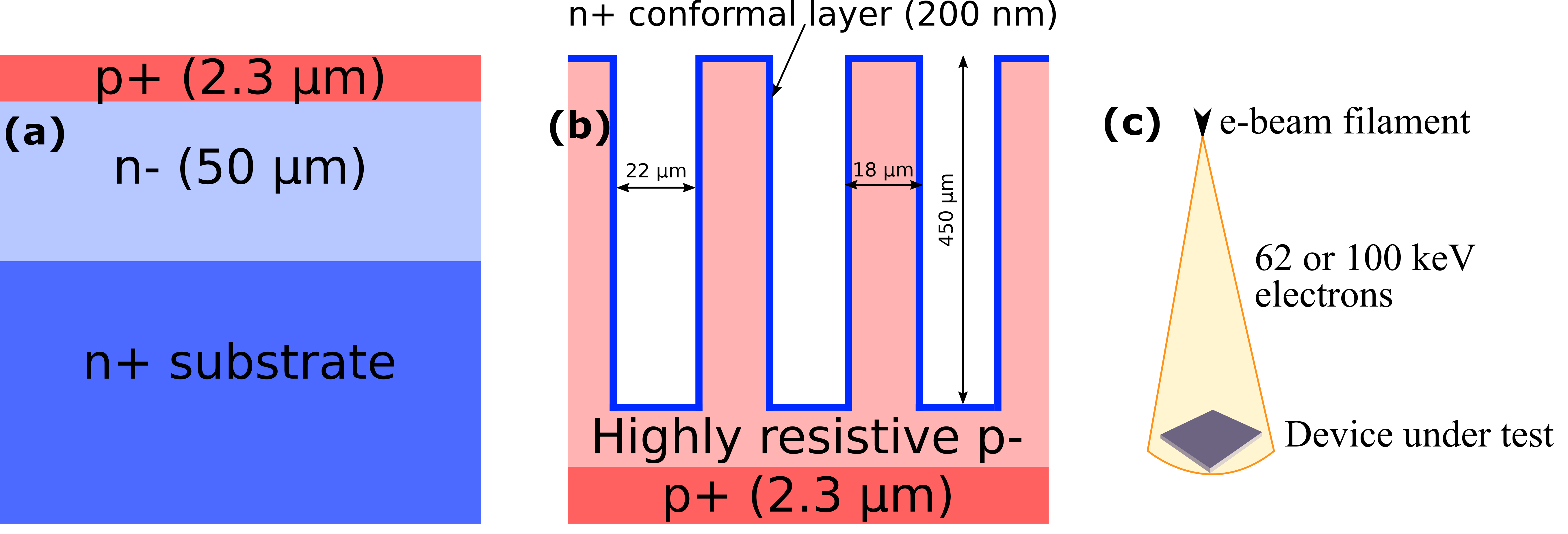
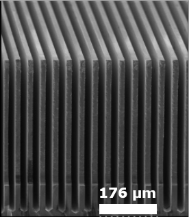
The silicon device was a 3D ridge p-i-n diode, etched into ridges 18 microns wide, 22 microns apart, and 450 microns deep, with a conformal p-type layer on the sidewalls to fully deplete the ridges. The 3D geometry is there to pack more source-to-junction interface into a given footprint, which is a power-density story, not a radiation story. Under 100 keV electrons at the same beam current density that damaged the SiC, the silicon diode showed no power degradation out to 7 x 10^18 cm^-2. Short-circuit current, open-circuit voltage, and fill factor were unchanged, and the dark current-voltage and capacitance-voltage curves before and after were indistinguishable, meaning no significant trap density formed. 100 keV is well short of the 250 keV needed to displace silicon, so the lattice simply does not register the dose.
 hover / hold for original
The caveat on the conclusion
One honest limit: our beam topped out at 100 keV, and the Pm-147 endpoint is 225 keV, so the highest-energy 30% of the real spectrum sits in a window we did not test. Those betas can in principle displace silicon, at least the ones above 200 keV, and the right follow-up is to push the accelerated aging up toward 225 keV and see whether silicon's advantage holds across the full spectrum. What the data support cleanly is the 100 keV comparison, and there silicon wins.
For a Pm-147 betavoltaic the practical reading is that silicon is the better converter, and not only on radiation hardness. It is commercially available, high quality, cheap, and the 3D fabrication processes are mature, which is exactly where SiC sidewall doping is still weak. The lesson I take from this is narrower and more useful than "wide bandgap is rad-hard." Radiation hardness is not only a property of the material, it is a property of the material against a specific spectrum given a specific geometry. Match the threshold to the source. For low-energy betas like Pm-147, the carbon sublattice that makes SiC interesting is the same thing that makes it fail. There is even the possibility that high-aspect ratio 3-d microstructured materials may have enhanced radiation hardness due to the possiblity that mobile defects can migrate to the surface and annihilate before they have the chance to combine and become immobile permanent electrical defects
The rest of the LLNL-era betavoltaic work is on my Google Scholar.