Picking a Detector Material with Monte Carlo
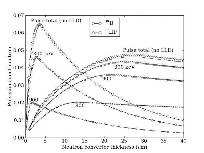
If you are building a solid-state thermal neutron detector and you only optimize one number, optimize the converter, not the semiconductor. With a 2.8 micron B-10 film the absolute ceiling on intrinsic thermal neutron detection efficiency is about 6.5% with no discriminator, and about 4.5% once you apply a realistic 300 keV lower-level discriminator. That ceiling is set almost entirely by the converter physics, and it is the same ~4.5% for a 26 micron Li-6 (as LiF) film. The semiconductor choice then decides how thin you can make the diode, how cheaply you can deplete it, and how well it ignores gamma background. This post lays out the framework I used to make those two choices in my dissertation work at UT-Dallas, advised by Profs. Bruce Gnade and Manuel Quevedo-Lopez. The numbers below all come from MCNP5 and MCNPX v2.7.0 simulations, cross-checked against devices we fabricated.
A solid-state thermal neutron detector is two layers stacked together. A converter layer absorbs a neutron and emits charged particles by a nuclear reaction, and a semiconductor diode underneath stops those charged particles and turns their energy into a measurable electrical pulse. Thermal neutrons (about 0.026 eV) carry far too little energy to ionize anything directly, so without the converter there is no signal at all. The whole material-selection problem reduces to two questions: which converter makes the most useful charged particles, and which semiconductor catches them with the least gamma sensitivity and the least fabrication pain. If you want the broader detector landscape first, I wrote that up separately in neutron detectors.
Step 1: pick the converter
There are only a handful of isotopes with a large enough thermal neutron capture cross section to be worth using, and an even smaller set that emit charged particles instead of just gamma rays. The candidates worth knowing:
| Isotope | Reaction | Thermal cross section (barns) | Charged products (keV) | Emits gammas? |
|---|---|---|---|---|
| He-3 | He-3(n,p)H-3 | 5333 | p: 573, H-3: 191 | No |
| Li-6 | Li-6(n,alpha)H-3 | 940 | H-3: 2727, alpha: 2055 | No |
| B-10 | B-10(n,alpha)Li-7 | 3835 | alpha: 1472, Li-7: 480 | Yes (478 keV) |
| nat-Gd | nat-Gd(n,gamma) | 49700 | conversion e-: 29-191 | Yes |
| U-235 | U-235(n,f) | 681 | fission products | Yes |
He-3 has the highest cross section of the gas-free options, but it is a gas, which rules it out for a thin solid film. That leaves the two practical solid converters, B-10 and Li-6, and they trade off in opposite directions. B-10 has a large cross section (3835 barns) so a thin film captures plenty of neutrons, but the reaction Q-value splits into a low-energy alpha (1472 keV) and a Li-7 recoil (480 keV). Li-6 has a much smaller cross section (940 barns) so it needs a thicker film to capture the same fraction of neutrons, but its reaction dumps a full 4.78 MeV into just two particles, a 2.05 MeV alpha and an energetic 2.73 MeV triton.
That energy difference is the reason the optimal thicknesses come out so different. The converter cannot be made arbitrarily thick, because the charged particles have to escape the film and reach the diode, so beyond some thickness you are absorbing neutrons in a region whose products self-absorb before they can produce a pulse. Sweeping film thickness in MCNPX, the efficiency peaks at about 2.8 microns for B-10 and about 26 microns for Li-6 at a 300 keV discriminator. The high-cross-section, low-energy converter wants to be thin, and the low-cross-section, high-energy converter wants to be thick.
 hover / hold for original
There is a second reason to care which converter you pick, and it shows up only when you account for the dead layer. Every real device has a thin dead layer between the converter and the active diode volume, typically about 100 nm of metal contact or heavily doped semiconductor, where deposited energy never becomes signal. A normally incident B-10 alpha or Li-7 ion in the 0.3 to 1.5 MeV range loses roughly 30 to 50 keV crossing 100 nm of aluminum, which is enough to drop the predicted efficiency from about 4.6% to about 4.2% by effectively pushing the discriminator up to ~350 keV. A 1 MeV triton from the Li-6 reaction loses only about 10 keV through the same dead layer. So Li-6 is more forgiving of the dead layer, because its products are more energetic and the same lost slice of energy is a smaller fraction of the total. The flip side is that B-10 emits a 478 keV gamma the Li-6 reaction does not, which is a strike against it for gamma rejection. Neither converter is strictly better, and which one wins depends on whether dead-layer losses or gamma cleanliness dominates your design.
Step 2: pick the semiconductor
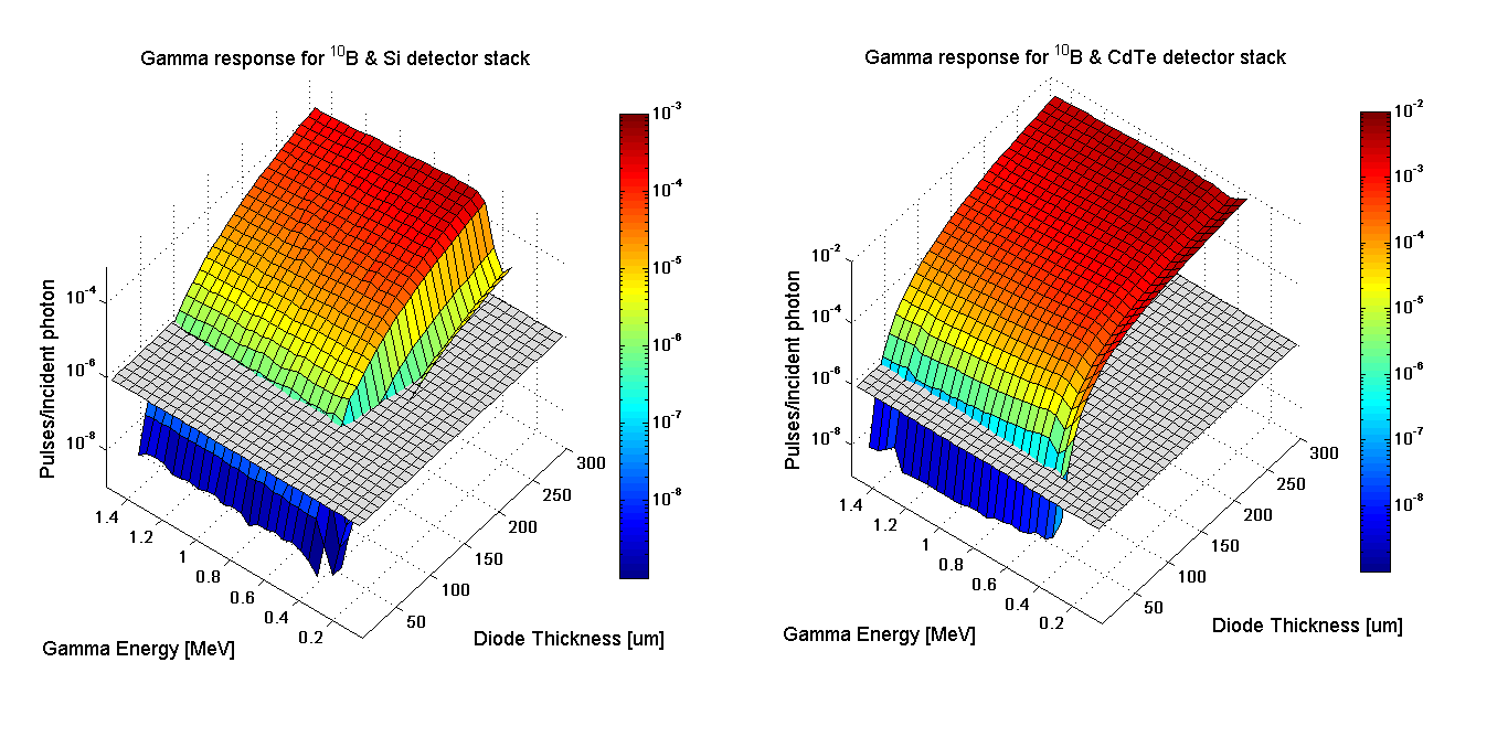
Once the converter is fixed, the diode question is how thin the semiconductor can be while still stopping the charged particles. Thinner is better for three independent reasons: it is cheaper, it is easier to fully deplete, and (the big one) it is far less sensitive to gamma background. The reason a thin diode rejects gammas is geometric. A Compton or photoelectric electron from a background gamma needs path length in the active volume to deposit enough energy to clear the discriminator, and a few-micron diode simply does not give it that path length, while the converter's charged particles stop in well under a micron and deposit their full energy regardless.
The minimum diode thickness to reach maximum neutron efficiency depends on the stopping power of the semiconductor for these specific ions. Sweeping diode thickness in MCNPX for a 2.8 micron B-10 converter at a 300 keV discriminator, the materials sort by how dense their electron cloud is:
| Semiconductor | Thickness for max efficiency | Max diode thickness for gamma rejection, B-10 | Max diode thickness for gamma rejection, LiF |
|---|---|---|---|
| Diamond (C) | ~0.6 micron | 60 micron | 49 micron |
| ZnO | ~0.7 micron | 36 micron | 31 micron |
| GaAs | ~1.0 micron | 38 micron | 30 micron |
| Si | ~1.3 micron | 86 micron | 74 micron |
| CdTe | ~1.3 micron | 28 micron | 27 micron |
The "max efficiency" column is the floor: below it the diode is too thin to absorb the charged particle's full energy. Diamond and ZnO have the highest stopping power and need only about half the thickness of silicon to absorb the same energy, which is why they reach maximum efficiency at ~0.6 and ~0.7 microns. The "max thickness for gamma rejection" columns are the ceiling, the thickest the diode can be while keeping the intrinsic gamma-neutron efficiency at or below the radiation-portal-monitor standard of 1e-6 (the spec that a gamma should almost never fake a neutron count). Silicon has by far the most generous ceiling, 86 microns, because its low atomic number makes it a poor gamma absorber. Counterintuitively diamond, despite being the lightest atom, has a smaller ceiling than silicon because its atomic density is so high that its electron density actually exceeds silicon's.
 hover / hold for original
The good news from both columns is that the floor (~1 micron) sits well below the ceiling (~30 to 86 microns), so there is a wide thickness window that is simultaneously fully efficient and effectively gamma-blind. For diodes at or below 10 microns, all five materials are basically gamma-blind at a 300 keV discriminator, even running 1e9 particle histories with forced-collision variance reduction it was hard to record a non-zero gamma tally. That is the strong argument for thin-film charged-particle detectors over thick bulk diodes.
One more constraint ties the thickness back to the material: you can only run a pulse out of the part of the diode you can deplete, and the depletion width depends on carrier concentration. Using the one-sided junction approximation, a carrier concentration around 1e16 cm^-3 gives about a 700 nm depletion width at 5 V reverse bias, which is just enough to absorb 300 keV from the B-10 products. That sets a real materials target: you want a semiconductor you can grow with a carrier concentration low enough to deplete past a micron at a modest bias. For polycrystalline thin films of CdTe and ZnO this is the hard part, and it is where the simulation framework hands off to fabrication reality.
Cross-checking against real devices
The framework is only worth something if the devices behave. We fabricated diodes from Si wafers and from thin films of both ZnO and CdTe and measured their alpha and neutron response. The result that mattered most: thin-film CdTe:CdS diodes produced a significant and reproducible electrical pulse from a single alpha particle, reported for the first time, which is the threshold capability a converter-coupled detector needs. The Si diodes and the thin-film work together confirmed the simulated picture, that a few-micron diode under a thin converter is enough to register single charged particles while staying blind to gammas. The full device data, including the CdTe:CdS pulse-height spectra, is in the dissertation and on my Google Scholar. The ZnO, while ideal in theory, cheap to fabricate, and capable of forming a rectifying junction, did not have the sensitivity required to detect individual alpha particles.
If you would like to see some of the simulation machinery underneath all of this: the pulse-height tally, variance reduction, and why the error bars are the actual result, that is in Monte Carlo radiation transport. The material framework is what turns those simulations into a decision: fix the converter for the efficiency ceiling, then pick the semiconductor for the thickness window that keeps you efficient, depletable, and gamma-blind all at once.